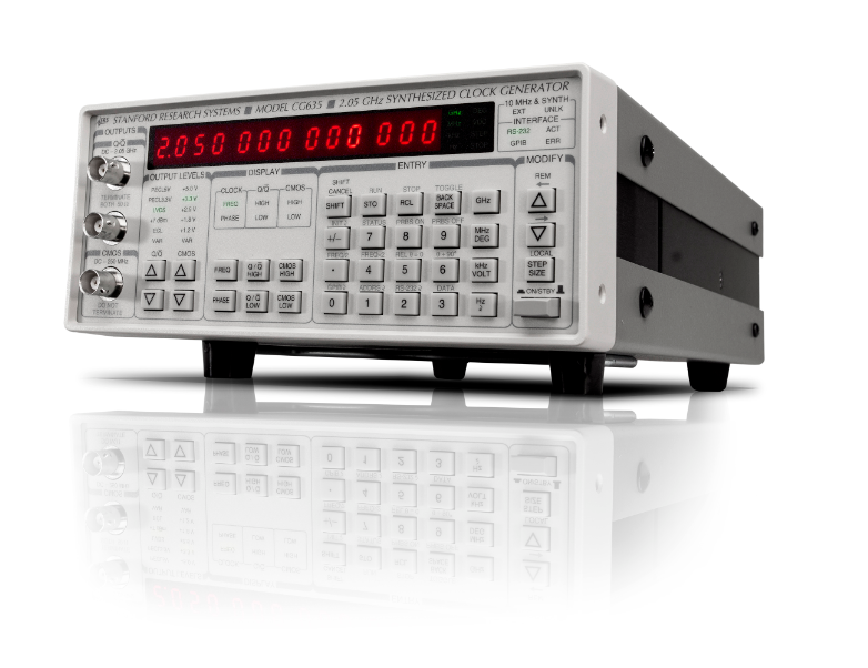
SRS CG635 Clock Generator,Stanford research systems CG635时钟发生器
CG635产生极为稳定频率范围从1μHz到2.05GHz的方波时钟。该仪器具有高频率分辨率,低抖动,快速转换时间和灵活的输出电平等特点使之成为任何数字元件、系统或网络测试的最理想选择。
·时钟频率1μHz到2.05GHz
·随机抖动<1 ps rms
·16位频率分辨率
·80 ps的上升和下降时间
·CMOS,PECL,ECL,LVDS,RS – 485的输出
·相位控制和时间调制
· OCXO and rubidium时基(选配)
CG635 Stanford research systems Clock Generator Specifications | |
Frequency | |
| Range | DC, 1 µHz to 2.05 GHz |
| Resolution | 16 digits (f ≥ 10 kHz), 1 pHz (f < 10 kHz) |
| Accuracy | Δf < ±(2 × 10-19 + timebase error) × f |
| Settling time | <30 ms |
Timebase (20 °C to 30 °C ambient) | |
| Stability | <5 ppm (std. timebase) <0.01 ppm (opt. 02 OCXO) <0.0001 ppm (opt. 03 Rb timebase) |
| Aging | <5 ppm/year (std. timebase) <0.2 ppm/year (opt. 02 OCXO) <0.0005 ppm/year (opt. 03 Rb timebase) |
| External input | 10 MHz ± 10 ppm, sine >0.5 Vpp, 1 kΩ |
| Output | 10 MHz, 1.41 Vpp sine into 50 Ω |
Phase Noise (at 622.08 MHz) | |
| 100 Hz offset | <-90 dBc/Hz |
| 1 kHz offset | <-100 dBc/Hz |
| 10 kHz offset | <-100 dBc/Hz |
| 100 kHz offset | <-110 dBc/Hz |
Jitter and Wander | |
| Jitter (rms) | <1 ps (1 kHz to 5 MHz bandwidth) |
| Wander (p-p) | <20 ps (10 s persistence) |
Time Modulation (rear-panel input) | |
| Input impedance | 1 kΩ |
| Sensitivity | 1 ns/V, ±5 % |
| Range | ±5 ns |
| Bandwidth | DC to greater than 10 kHz |
Phase Setting | |
| Range | ±720° (max. step size ±360°) |
| Resolution | <14 ps |
| Slew time | <300 ms |
Q and −Q Outputs | |
| Outputs | Front-panel BNC connectors |
| Frequency range | DC to 2.05 GHz |
| High level | -2.00 V ≤ VHIGH ≤ +5.00 V |
| Amplitude | 200 mV ≤ VAMPL ≤ 1.00 V (VAMPL ≡ VHIGH – VLOW) |
| Level resolution | 10 mV |
| Level error | <1 % + 10 mV |
| Transition time | <100 ps (20 % to 80 %) |
| Symmetry | <100 ps departure from nominal 50 % |
| Source impedance | 50 Ω(±1 %) |
| Load impedance | 50 Ω to ground on both outputs |
| Preset levels | PECL, LVDS, +7 dBm, ECL |
CMOS Output | |
| Output | Front-panel BNC |
| Frequency range | DC to 250 MHz |
| Low level | -1.00 V ≤ VLOW≤ +1.00 V |
| Amplitude | 500 mV ≤ VAMPL ≤ 6.00 V (VAMPL ≡ VHIGH – VLOW) |
| Level resolution | 10 mV |
| Level error | <2 % of VAMPL+ 20 mV |
| Transition time | <1 ns (20 % to 80 %) |
| Symmetry | <500 ps departure from nominal 50 % |
| Source impedance | 50 Ω (reverse terminates cable reflection) |
| Load impedance | Unterminated 50 Ω cable of any length |
| Attenuation (50 Ω load) | Output levels are divided by 2 |
| Preset levels | 1.2 V, 1.8 V, 2.5 V, 3.3 V or 5.0 V |
RS-485 Output | |
| Output | Rear-panel RJ-45 |
| Frequency range | DC to 105 MHz |
| Transition time | <800 ps (20 % to 80 %) |
| Clock output | Pin 7 and pin 8 drive twisted pair |
| Source impedance | 100 Ω between pin 7 and pin 8 |
| Load impedance | 100 Ω between pin 7 and pin 8 |
| Logic levels | VLOW = +0.8 V, VHIGH = +2.5 V |
| Recommended cable | Straight-through Category-6 |
LVDS Output (EIA/TIA-644) | |
| Output | Rear-panel RJ-45 |
| Frequency range | DC to 2.05 GHz |
| Transition time | <100 ps (20 % to 80 %) |
| Clock output | Pin 1 and pin 2 to drive twisted pair |
| Source impedance | 100 Ω between pin 1 and pin 2 |
| Load impedance | 100 Ω between pin 1 and pin 2 |
| Logic levels | VLOW = +0.96 V, VHIGH = +1.34 V |
| Recommended cable | Straight-through Category-6 |
PRBS (Opt. 01, EIA/TIA-644) | |
| Outputs | PRBS, -PRBS, CLK and -CLK |
| Frequency range | DC to 1.55 GHz |
| Level | LVDS on rear-panel SMA jacks |
| PRBS generator | x7 + x6 + 1 for a length of 27 – 1 bits |
| Transition time | <100 ps (20 % to 80 %) |
| Load impedance | 50 Ω to ground on all outputs |
General | |
| Computer interfaces | GPIB and RS-232 std. All functions can be controlled through either interface. |
| Non-volatile memory | Ten sets of instrument configurations can be stored and recalled. |
| Power | 90 to 264 VAC, 47 to 63 Hz, 50 W |
| Dimensions, weight | 8.5″× 3.5″ × 13″ (WHL), 9 lbs. |
| Warranty | One year parts and labor on defects in materials and workmanship |