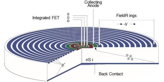
The working principle of the Silicon Drift Detector (SDD) is based on the concept of sideward depletion invented by Pavel Rehak and Emilio Gatti in 1983. It allows the depletion of a large volume of high-resistivity silicon material by a small anode receiving a minimum signal capacitance. By that, the SDD overcomes the major problem of a classical p-i-n diode detector where the input capacitance is direct proportional to the active area. Below figure shows a schematic view of the SDD in its standard configuration :
硅漂移探测器(SDD)的工作原理基于Pavel Rehak和Emilio Gatti于1983年发明的侧向耗尽概念。它允许通过接收最小信号电容的小阳极来耗尽大体积的高电阻率硅材料。通过这一点,SDD克服了经典p-i-n二极管检测器的主要问题,其中输入电容与有源面积成正比。下图显示了标准配置下SDD的示意图。

While the back contact is made up by a homogeneous, shallow p+n junction on the side where the incoming radiation enters the detector, the opposite side is characterized by a structure of circular p+ drift rings and eventually an integrated first FET for on-chip amplification. By applying a negative voltage on the radiation entrance window and an increasingly negative voltage on the drift rings, a potential field distribution is created such that the electrons generated by the ionizing radiation drift towards the small sized collecting anode situated in the center of the device. In the case of an integrated FET, the signal is directly amplified without adding any additional noise or microphony problems by bond wires.
虽然背接触由入射辐射进入探测器一侧的均匀浅p+n结组成,但相反一侧的特征是圆形p+漂移环的结构,以及最终用于片上放大的集成第一FET。通过在辐射入射窗上施加负电压并在漂移环上施加越来越负的电压,产生了电势场分布,使得由电离辐射产生的电子向位于器件中心的小尺寸收集阳极漂移。在集成FET的情况下,信号被直接放大,而不添加任何额外的噪声或键合线的微光学问题。
Key Features
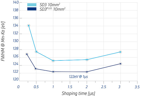
Best energy resolution down to 121 eV @ Mn-Kα, – 30°C
Polysilicon technology for ultra-low leakage current values < 100 pA/cm², enabling high performance spectroscopy close to room temperature
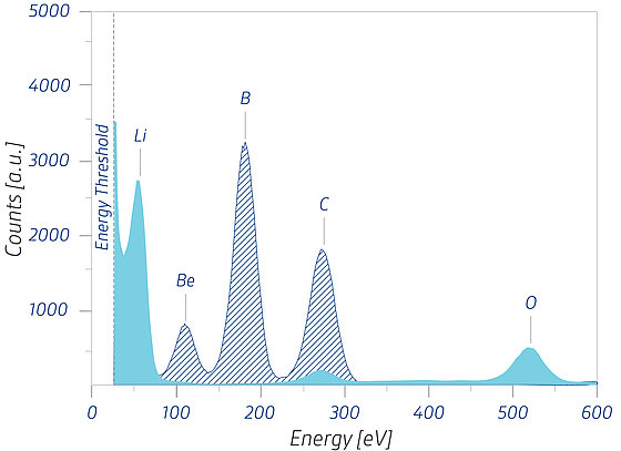
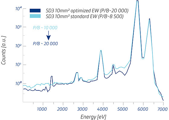
pnWindow for the best light element detection and optimum P/B ratio up to 20 000
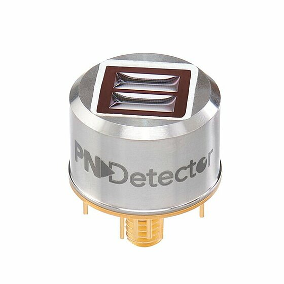
Wide selection of chip sizes and detector housings 5, 10, 20, 30, 60, 80, 100, 200, 300, 600 mm²
Unique shapes like our Rococo Series and the Rococo Detectors
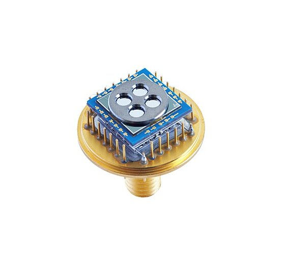
High count rates up to 1 Mcps with single cells and several Mcps with our monolithic Multi-Element SDDs
Radiation hardness >1014 Photons/cm²
主要功能
最佳能量分辨率低至121 eV@Mn-Kα,-30°C
超低漏电流值<100 pA/cm²的多晶硅技术,实现接近室温的高性能光谱
pnWindow可实现最佳的光元件检测和高达20000的最佳P/B比
广泛选择芯片尺寸和探测器外壳5、10、20、30、60、80、100、200、300、600 mm²
独特的形状,如我们的Rococo系列和Rococo探测器
单探测器高计数率高达1 Mcps,单片多元件SDD高计数率达数Mcps
辐射硬度>1014光子/cm²