的工作原理")
硅漂移探测器Silicon Drift Detector (SDD)的工作原理
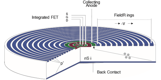
硅漂移探测器(SDD)的工作原理 The working principle of the Silicon Drift Detector (SDD) is based on the concept of sideward depletion invented by Pavel Rehak and Emilio Gatti in 1983. It allows the depletion of a large volume of high-resistivity silicon material by a small anode receiving a minimum signal capacitance. By that, the SDD overcomes the major problem of a classical p-i-n diode detector where the input capacitance is direct proportional to the active area. Below figure shows a schematic view of the SDD in its standard configuration : 硅漂移探测器(SDD)的工作原理基于Pavel Rehak和Emilio Gatti于1983年发明的侧向耗尽概念。它允许通过接收最小信号电容的小阳极来耗尽大体积的高电阻率硅材料。通过这一点,SDD克服了经典p-i-n二极管检测器的主要问题,其中输入电容与有源面积成正比。下图显示了标准配置下SDD的示意图。
Key Features
-
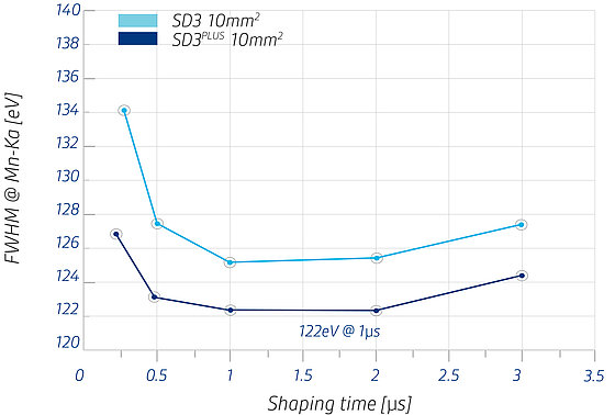
Best energy resolution down to 121 eV @ Mn-Kα, – 30°C
-
Polysilicon technology for ultra-low leakage current values < 100 pA/cm², enabling high performance spectroscopy close to room temperature
-
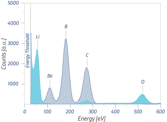
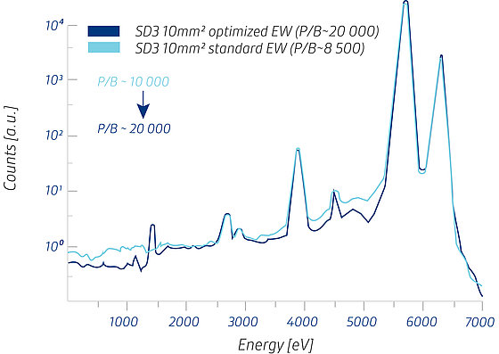
pnWindow for the best light element detection and optimum P/B ratio up to 20 000
-
Wide selection of chip sizes and detector housings 5, 10, 20, 30, 60, 80, 100, 200, 300, 600 mm²
-
Unique shapes like our Rococo Series and the Rococo Detectors
-
High count rates up to 1 Mcps with single cells and several Mcps with our monolithic Multi-Element SDDs
-
Radiation hardness >1014 Photons/cm²
询价采购硅漂移探测器Silicon Drift Detector (SDD)的工作原理
请用微信扫描下方二维码或手动添加微信号2351992198


的工作原理")